-
Home

- Uncategorised
Uncategorised
eLitho Extension Line
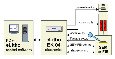
The lithography systems of the eLitho extension line are comprehensive, high performance add-on modules for commercial microscopes (SEM, FIB, STEM, TEM, multi-beam). They are easy to use and provide a broad variety of expedient definitions with respect to electronics and software complexity. All realizations are based on the layout-editor eDraw for the structure design and the eLitho control software for supervising the lithography process. Thus virtually every scanning microscope can be utilized to achieve a perspicuous, multi-functional nanolithography unit.
- eDraw CAD layout editor
- eLitho Exposure-control and documentation software
- Software modules increase the potential of the software due to sophisticated tasks
 nanonic offers a wide variety of pertinent high quality hardware models for electron beam and FIB lithography:
- EK 3000 universal 19” comprehensive lithography unit
- EK 3100 high performance providing a 50% higher maximum writing speed
- EK 3000²/EK 3100² special systems for controlling two beam system (SEM/FIB)
- EK 5000/EK 5000² high end lithography system for ambitious applications
All hardware models utilize progressive DSP-based electronics, which are specially designed to fit in the potentials of the used machine.
In order to satisfy possible additional requirements as for a capable running lithography system we offer several useful hardware accessories for the eLitho system.
We are looking forward to an on site demonstration of our systems. Please do not hesitate to contact us.
Hardware
The progressive DSP-based hardware is specially designed to fit in the potentials of the used machine. We provide three systems. The EK 3000 system is an universal economic lithography electronics for nearly all SEM or FIB systems. For higher deflection speed the EK 3100 system is available. The high performance EK 5000 hardware has been developed to use in all respects the full capacity of state-of-the-art machines.
Here we present some features of our hardware components:
|
|||||
|
|||||
|
|||||
|
|||||
|
|||||
|
| EK 2000 | EK 3000 | EK 3100 | EK 5000 | ||
|
2.7 MHz | 5.0 MHz | 7.5 MHz | 12 MHz | |
|
16 ns | 13 ns | 13 ns | 3 ns | |
|
2048 | 6144 | 12288 | 32768 |
|
||||
| EK 2000 | EK 3000 | EK 3100 | EK 5000 | |
| 2.7 MHz | 5.0 MHz | 7.5 MHz | 12 MHz | |
|
||||
| EK 2000 | EK 3000 | EK 3100 | EK 5000 | |
| 16 ns | 13 ns | 13 ns | 3 ns | |
|
||||
| EK 2000 | EK 3000 | EK 3100 | EK 5000 | |
| 2048 | 6144 | 12288 | 32768 | |
Service
Our default service includes:
- substantial guidance as for acquisition of a lithography-establishment
- adaptation to SEM, STEM or FIB
- on site installation and user training
Due to a steady improvement of our products specifications are subject to change without notice.
Company background
nanonic is an ambitious and capable company working in the innovative field of nanolithography. It was founded by a group of Ph. D. students in the workgroup of Prof. Dr. Dieter Weiss at the University of Regensburg. We were engaged in physics of semiconductor and metallic nanostructures and initiated our first EBL-Software in 1997. Within a short time we expanded the software with regard to image capture and manual structure alignment. In 2000 we began with the development of our own graphical layout-editor and integrated several useful software add-ons. Since 2002 we have been developing the new extensive nanonic eLitho Lithography-System, integrating a variety of high capacity electronics and a sophisticated software package. Our scientific background and the practical work with nanostructures provide us with a lot of incitation for the continual improvement of our systems.
Furthermore, we have established useful contacts to the leading SEM and FIB manufacturers throughout this period, which is especially important for the adaptation and the remote controlling of the microscopes and the development of machine enhancements.
Corporate information
Responsible for the internet pages of nanonic GmbH
